Understanding how a device's firmware work could be helpfull for many activities: to discover features that you were not aware of, to find the way to enable a device feature you should otherwise paid for, to discover how to install an alternative firmware, to conduct a security audit, etc.
You can also do this to identify the cause of a strange failure in a device as it provides the full picture of a device operation priciple from a logic point of view. This is the case of the Briot Tracer as this was my first contact with this device and I had absolutelly no clue how it operates or what its normal behaviour is.

In this post I will use the Briot Tracer as an example to show (at least partially) the firmware reverse engineering process and what information we can expect from it. It is selected as it uses an external memory (EPROM type) so the process of obtaining the firmware is straight forward, in other cases the process required to obtain the firmware could me more complicated.
 |
Before starting let me clarify that under no circumstances I am going to publish, share or distribute the firmware of this device. If you contact me asking for the firmware I will not even reply. I am going to show some small pieces of disasembled code only with the purpose of explaining something or making a point. |
Firmware Reverse Enginnering Process
The process of obtaining the firmware could be very simple as in this case in which you just take the memory IC out of the DIP socket and connect it to a programmer to read its contents. In other cases it could be extremelly complex and require more advanced techniques as clock or power glitching with the objective of getting the content of the internal (protected) memory flash, or the process to find the encryption scheme and the key to decrypt the firmware.
This example could be seen as a simple complete case of the firmware reverse engineering process (starting from obtaining the firmware from the electronic circuit) without going into the required steps to circumvent the flash memory protections of more modern microcontrollers.
Despite such memory protection capabilities of modern microcontrollers there are still manufacturers that ships their products with such protection disabled, making their products prone to being copied by inescrupolous parties. (More on this in a future post)
The general steps are:
- Create a minimal circuit schematic containing the main components. To understand what the firmware wants to achieve when, for example, puts a high level on an output pin. Also is needed in some cases like this one to ceate the I/O and memory map as the corresponding memory addresses are hardware defined.
- Create a memory and input/output map.
- Obtain the device firmware.
- Disassemble the firmware. Convert the binary machine code (most of the times incorrectly called assembly) into assembler and/or a higher level code like C.
- Analyze the disassembled code. Put every piece together in order to understand what the device is trying to do.
The complete Briot Tracer schematic was presented in a previous post as a PDF file. Please consider taking a look at it to be able to easily understand what follows.
Memory and Input/Output Map
In a modern microcontroller based device, the memory (typically FLASH and RAM) and peripherial I/O address map is hardcoded in its internal silicon design. In the case of the device under analysis such memory map must be constructed based on the schematic and the information provided by the microcontroller manufacturer in the datasheet. In both cases is needed to analyze the schematic to identify what purpose is serving each one of the microcontroller pins, or at least the most relevant ones.
In this case the microcontroller is an NXP 80C552, a 8051 based device with some embedded peripherials, like UART, ADC, Timer and I2C among others.
The following information can be extracted from the circuit schematic and the microcontroller datasheet to construct the memory and I/O map:
- The EA input pin of the 80C552 is permanently tied to ground so it only executes code from external memory.
- The 80C552 has a 16-bit address and 8-bit data buses so it can address 64Kb x8 of external memory from 0x0000 to 0xFFFF. It can also address 64Kb x8 of external RAM memory from 0x0000 to 0xFFFF.
- U22 is an 74HC138 (3-to-8 line decoder/demultiplexer) and it defines the I/O addresses at which the external ICs are accessed, its active low output enable signals are active at addresses 0x8000 to 0x80E0 in 0x20 jumps. (As no full decoding is used multiple aliases of each address exists)
If you look carefull you will notice something odd. The external memory used is a 27C1001 which is actually double the memory (128Kb x8) that the 80C552 can address (64Kb x8). So Briot has choosen to spend more money in a bigger than needed memory, why?
The answer is to provide two different firmwares in one single memory IC. One for normal operation and one for testing (probably). In page 6 of the schematic you can see that they have connected A16 of the external EPROM to a jumper and a pull-up resistor. This way changing the jumper position you can choose to execute the code in the upper (from 0x10000 to 0x1FFFF) or lower (0x0000 to 0xFFFF) 64Kb of memory of the memory IC. In both cases the memory is mapped to the microcontroller address range 0x0000 to 0xFFFF.
In the following image the memory and input/output map is presented.
 |
| Briot Tracer - Memory and I/O Map |
There are some GPIO of the microcontroller that serve some specific purposes. In the page 4 of the schematic there is a list of the microcontroller ports signal purpose, in the following image I present that same list. On each line the microcontroller PortNumber.Bit and direction (I for Input and O for Output) on the left and the purpose on the right, except for the dedicated PWM signals.
 |
| Briot Tracer - Microcontroller GPIO Purpose |
Finally, U23 adds some more GPIO pins that manages other functions. In the page 7 of the schematic there is a list of the programmable peripherial interface ports signal function, in the following image we present that same list.
 |
| Briot Tracer - Programmable Peripherial Interface Ports Pins Purpose |
Firmware Disassembling, Ghidra
A couple of years ago the National Security Agency (NSA) has published Ghidra, which is a powerfull tool for software reverse engineering. In this section I am going to present the steps followed from the importation of the binary file to obtaining the full disassembled code. In this case there are some required extra steps that deviates from the typical workflow, for examaple the creation of specific memory blocks to represent the I/O access memory addresses.
To avoid visual poluttion some detailed steps are presented in a collapsible section.
The first step is to create a Ghidra project. After creating the project it is necessary to import the file containing the binary code. This can be done by dropping the binary file in the Ghidra window or from the menu: File -> Import and selecting the binary file. The following image shows the result after selecting the file to import.
 |
| Briot Tracer - Ghidra Import Source |
The next step is the selection of the processor or processor family for which the code was compiled, in this case 8051. The following image shows the processor-variant-compiler combination selected in this case.
 |
| Briot Tracer - Ghidra Import Select Microcontroller |

|
In some cases the imported binary file already contains the processor family information so this step is performed automatically. This is the case, for example, when opening an ELF file, because the ELF header structure has the value e_machine which contains this information. For example, for ARM this value is set to EM_ARM (ARM ELF File Format). |
After selecting the processor family, in the Options button you can verify, or change, some parameters related to the location of the code in memory: the base address, the file offset and the length of the code. In this case I have changed the block name to "ROM". This allows to quickly identify the code block in the ghidra disassembler.
 |
| Briot Tracer - Ghidra Import Code Block Options |
Now you can import the code by clicking the OK button in the import window.
 |
| Briot Tracer - Ghidra Import Ready to Import the Code |
After the code is imported ghidra presents an import result summary. Some items to pay attention to are: # of Bytes, Minimum Address and Maximum Address. In this case # of Bytes should be 65535, since the code is 64Kb long. The difference is because the addressable registers are also considered.
 |
| Briot Tracer - Ghidra Import Results Summary |
The import process is now finished, use the OK button to go back to ghidra main screen.
To disassemble the code you need to open the CodeBrowser tool. You can do this by double-clicking on the corresponding ".bin" file name, using the menu, or using the green dragon icon in the Tool Chest. Now you can, if you want, run the code analysis tool. In the following image you can see the CodeBrowser window after double-clicking on the ".bin" file name, asking whether or not you want to run the code analysis tool.
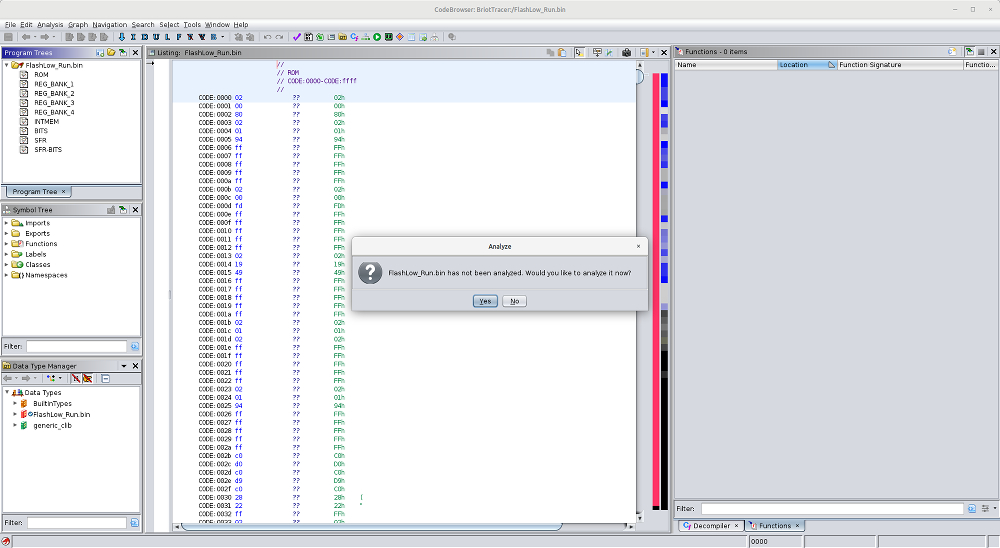 |
| Briot Tracer - Ghidra CodeBrowser Initial Window |
Before you disassemble the binary code you must define the memory blocks for RAM and I/O in the ghidra memory map. This will help to understand the disassembled code since the corresponding names for these blocks are used in the disassembled code.
To open the memory map you can use the corresponding icon in the toolbar (the one that looks like a small SODIMM RAM module) or use the menu: Window -> Memory Map. The following image shows the Memory Map window.
 |
| Briot Tracer - Ghidra CodeBrowser Memory Map |
If you want, you can change the access permission to the ROM memory block by clicking on the corresponding checkbox, you can see in the previous image that it is marked as writable ("W"), which is not correct. In these options, the "X" indicates that the processor can execute code from this memory block.
Now you can create the RAM and I/O memory blocks. All the memory blocks to be created are of type EXTMEM. You can see in the following images the data used to create each one.
 |
| Briot Tracer - Ghidra Memory Map RAM Block |
 |
| Briot Tracer - Ghidra Memory Map I/O PPI Block |
The IO_ROT memory block can only be written, since none of the stepper motor controller registers can be read.
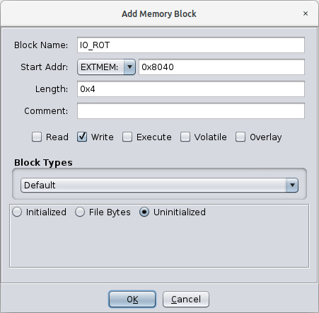 |
| Briot Tracer - Ghidra Memory Map I/O Rotation Block |
 |
| Briot Tracer - Ghidra Memory Map I/O RS232 Block |
The IO_QENC memory block can only be read, since none of the stepper motor controller registers can be written.
 |
| Briot Tracer - Ghidra CodeBrowser Memory Map I/O Quadrature Decoder Block |
The following image shows the memory map after adding all the memory blocks.
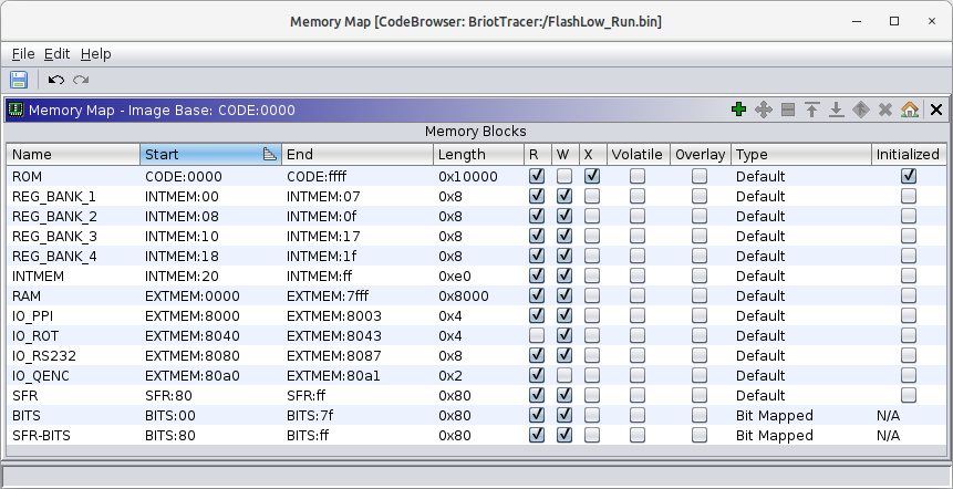 |
| Briot Tracer - Ghidra Finished Memory Map Blocks |
Now it is time to analyze the code, if you chose not to do so when importing the binary file. In the following image you can see the Analysis Options window with the default options. You can re-run the code analysis from the menu: Analysis -> Automatically analyze 'filename' or by pressing the A key on your keyboard.
 |
| Briot Tracer - Ghidra Binary Code Analisys |
|
|
The other times I have used Ghidra, for example with ELF files containing code for ARM processors, when the analysis of a file is performed it automatically disassembles all the code. In this case for some reason it does not. To disassemble the ROM binary data, select the entire contents in the Listing view and press the D key on the keyboard, or right-click the mouse in the Listing view and select the Disassemble option. |
In the following image the main window of Ghidra with the already disasembled code is presented.
 |
| Briot Tracer - Ghidra CodeBrowser Main View |
There is one more step before starting to analyze the disassembled code. Since Briot Tracer uses a derivative of the 8051, it contains registers that the Ghidra 8051 definition does not know about. You can use the 80C552 datasheet to correct the labels of these registers. An example can be seen in the following image for the register at address 0x84 which is labeled as DPXL. Comparing the Ghidra labeling with the datasheet (Page 56, Figure 44) you can see the difference, there is no register in the 80C552 at address 0x84.
 |
| Briot Tracer - Ghidra Special Function Registers |
To correct the labels right-click and select the Edit Label option, or press the L key on the keyboard while the cursor is over the desired register, and enter the desired label in the text field.

|
Correcting the register labels is not necessary, after all they are just labels, but it helps to correctly understand what the firmware is trying to do when it writes a certain value to a register. |
In a future post I will show how to identify some important functions and their principal purpose, stay tuned.
No comments:
Post a Comment